

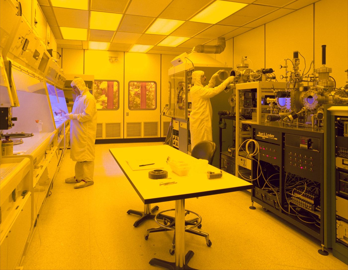
Inside a semiconductor factory, some of the most precise work happens invisibly, as gases etch patterns into silicon wafers with features far smaller than a human hair. Those process gases are expensive, tightly controlled and in some cases potent greenhouse gases, so engineers are now testing revised dry etching recipes that achieve the same precision while using substantially less gas per wafer. The approach relies on tighter plasma control, real-time sensors and pulsed delivery, applying gas only in the exact moments and quantities the reaction requires rather than in a continuous flow. For chip makers facing both environmental reporting pressure and volatile supply costs, the savings could be significant across millions of wafers. Crucially, the trials are being run on production-grade equipment rather than laboratory benches, measuring not only gas consumption but also defect rates, uniformity across the wafer and throughput, because no saving is worthwhile if it lowers the yield of working chips from each expensive production run. Early adopters expect the savings to compound as sensor prices fall and recipes are shared industry-wide.
What the Evidence Shows
Results so far suggest the leaner recipes can match conventional quality on several common etching steps, particularly where sensor feedback allows the plasma to adjust itself hundreds of times per second. Engineers say the data collected is valuable in itself: detailed records of how each wafer responds help process teams spot drift earlier and reduce wasted runs. Environmental specialists note that semiconductor manufacturing has a concentrated footprint, so improvements inside a single large plant can deliver outsized reductions compared with dispersed industries. The challenge now is qualification, since customers in automotive, medical and aerospace sectors require lengthy validation before any process change reaches their components. Manufacturers expect a gradual rollout, step by step and product by product, rather than a sudden switch. Even so, the direction is clear: the future competitiveness of chip plants will be judged not only on how small their transistors are, but on how cleanly and efficiently they can make them. Reporting and analysis from sources such as MIT Technology Review track the same developments, and specialists following the low-gas dry etching process say the direction is now consistent across independent lines of evidence.
The Wider Context
The wider context is an industry learning to ship capability and restraint together. Products built around the low-gas dry etching process now launch with safety evaluations, usage data and rollback plans as standard, because enterprise buyers and regulators ask for them in the first meeting. Companies that treated those questions as friction are discovering they have become the purchase criteria.
What Happens Next
What happens next for the low-gas dry etching process depends less on another breakthrough than on the unglamorous work of reliability, pricing and support. The buyers evaluating it now are not enthusiasts; they are operators with budgets and auditors, and their checklists will decide the timeline. On the evidence of the current pilots, the technology has earned the right to be judged by them. You can follow related developments in our coverage of technology.
There is a practical lesson in all of this for readers deciding what to do today. Start with the verified facts, be wary of anyone promising certainty, and prefer reversible steps while the evidence is still developing. Circumstances differ by country, income and personal situation, so general guidance should always be weighed against your own context before you act on it in any significant or lasting way.
